All you need to know about GPIO on ADSP2192-12
(special guest : the GPIO interrupts !)
The ADSP2192-12 is equipped with eight GPIO (General Purpose Input Output) pins, that permit to connect the chip
to the external world.
Obviously, the ADSP2192-12 Hardware Reference Guide gives only a few informations about the GPIO port.
Some informations, like about GPIO interrupts, are missing, at least in the GPIO pages (GPIO interrupts are lightly evocated in PWRPx register description)
All informations given hereafter are expected to be exact (you know the disclaimer.. ░-)
Note : in all registers described hereafter, bit numbering is the same as GPIO pin numbering (eg : GPIOCFG:5 corresponds to GPIO5 pin)
All bits marked as 'R' are reserved
Configuring GPIO
The first 'level' of configuration is given by GPIOCFG register. This register selects the direction (input or output) of each GPIO pin.
| GPIOCFG (Reset = 0x7F)
|
| 15 | 14 | 13 | 12 | 11 | 10 | 9 | 8 |
7 | 6 | 5 | 4 | 3 | 2 | 1 | 0 |
| R | R | R | R | R | R | R | R |
D | D | D | D | D | D | D | D |
D : 0=Output - 1=Input
*** Note that GPIO7 is configured as an output at reset ! ***
For each output, it is possible to select either push-pull (called CMOS by Analog!) or open-drain configuration, by using GPIOPOL.
| GPIOPOL (Reset = 0xFF) |
| 15 | 14 | 13 | 12 | 11 | 10 | 9 | 8 |
7 | 6 | 5 | 4 | 3 | 2 | 1 | 0 |
| R | R | R | R | R | R | R | R |
P | P | P | P | P | P | P | P |
The function of P bits depends of the GPIOCFG and GPIOSTKY :
| GPIOCFGx |
GPIOSTKYx |
P bit function |
| 0 | X | 0=Push-pull output configuration
1=Open-drain output configuration |
| 1 | 0 | P bit has no action |
| 1 | 1 | 0=Input is 'sticked' to 1 when high
1=Input is 'sticked' to 1 when low |
To select 'sticky' bits, you need to program GPIOSTKY register
| GPIOSTKY (Reset = 0x00) |
| 15 | 14 | 13 | 12 | 11 | 10 | 9 | 8 |
7 | 6 | 5 | 4 | 3 | 2 | 1 | 0 |
| R | R | R | R | R | R | R | R |
S | S | S | S | S | S | S | S |
S : 0=Not sticky(normal input) - 1=Sticky bit
Writing GPIO outputs
To set the state of a GPIO output pin, write the desired state of the pin in the corresponding GPIOCTL bit.
| GPIOCTL (Reset = GPIO pins state at power-on)
|
| 15 | 14 | 13 | 12 | 11 | 10 | 9 | 8 |
7 | 6 | 5 | 4 | 3 | 2 | 1 | 0 |
| R | R | R | R | R | R | R | R |
D | D | D | D | D | D | D | D |
Reading D : Power-On
Writing D : Set state of output pin
Note : Writing into the GPIOCTL bit of an input has no effect !
Reading GPIO inputs
The current state of all GPIO pins (inputs and outputs) is reflected in GPIOSTAT register.
Note that if a pin is configured as 'sticky', GPIOSTAT may return a state which is different of real state of the pin, if the input has been 'sticked'.
| GPIOSTAT (Reset = Depends on pin state...)
|
| 15 | 14 | 13 | 12 | 11 | 10 | 9 | 8 |
7 | 6 | 5 | 4 | 3 | 2 | 1 | 0 |
| R | R | R | R | R | R | R | R |
S | S | S | S | S | S | S | S |
Reading S : Pin state
Writing S : 0=No effect - 1=Clear Sticky Bit
Using GPIO sticky inputs
When configured as 'sticky', an input which goes to 'active' level (see GPIOPOL definition) is 'sticked' to this level, even if the GPIO pin goes back to the non-active state.
To clear a sticky input, you have to write a '1' in the corresponding bit of GPIOSTAT (yes, you clear with a '1', not a '0').
Note that clearing a 'sticky' input which corresponding GPIO pin is at active level has no effect (the bit remains 'sticked').
Using GPIO inputs as level sensitive interrupt inputs
With GPIO interrupts, we arrive at the non-documented side (well, it's rather bad-documented) of the ADSP2192-12.
If you read the data-sheet of the ADSP2192-12 (and some arrays of the Hardware Reference), you will notice that Interrupt 6 is reserved.
Now, take a look at table B-6 : you will notice that this interrupt is in fact dedicated to... GPIO (IMASK bit 6). Table E-1 gives the name of this interrupt : SYSTEM INTERRUPT.
If you activate Interrupt 6 with following code, you will notice that... nothing arrives, whatever the state of your GPIO inputs !
Here are the (secret ?) steps to follow to use GPIO interrupts :
- Route the Interrupt Vector 6 to your interrupt handler
- Set GPIOCFG as to create at least one input
- Declare the GPIO input you want to be an interrupt input as sticky, with GPIOSTKY
- DECLARE THE SAME GPIO INPUT AS WAKE-UP ENABLED WITH GPIOWCTL REGISTER
- Activate GPIO interrupt with GIEN bit (bit 10 of PWRP0 for core 0, and PWRP1 for core1)
Now, your DSP will jump to your interrupt handler each time the GPIO pin you choose goes to active level (depending of GPIOPOL)
There is no limitation in the number of GPIO inputs declared as Interrupt Inputs. In fact, since there is only one vector, all Interrupt Inputs are ORed inside the DSP.
In your interrupt handler, you have to do two things to clear the interrupt flag, otherwise the DSP will jump back to interrupt handler as soon as it will encounter the RTI instruction.
- 1 - clear the sticky bit by writing a '1' in GPIOSTAT corresponding bit
- 2 - clear GINT bit (bit 14 of PWRP0 register for core 0 and PWRP1 for core 1) by writing a '1' in it
You want an example project ??? Just click here...
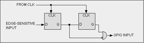
Using GPIO inputs as edge sensitive interrupt inputs
The ADSP2192-12 doesn't support edge sensitive interrupts. The GPIO interrupt is level sensitive,
meaning that if the input remains at active level, interrupt handler will be called as soon as the RTI
instruction is executed.
To support edge sensitive interrupts with ADSP2192, it is necessary to use a small amount of external logic.
The function of this logic is to transform a long duration logic level into a very short duration one, so that the input
will return to inactive state before GPIO interrupt is serviced.
The schematic given hereafter is an example of falling edge detector which can be used with the ADSP2192. On our prototype, we
implemented the circuit in a 16V8 GAL. The clock must be fast enough to generate sufficiently short pulses. You can get this
clock from AC'97 link SCLK line (12.288 MHz). A faster clock can also be used.
To obtain a rising edge detector, you have just to reverse the two inputs of the AND gate.
You can also build a dual-edge detector (GPIO interrupt on each edge) by replacing the AND gate with an Exclusive OR gate.
VERY IMPORTANT : Do not forget that the ADSP2192-12 can be powered from a 3.3V source. In this case, DO NOT CONNECT 5V POWERED
CIRCUIT (SUCH AS A GAL) DIRECTLY TO THE DSP. It may destroy it !!!
In this case, you can use 5V/3.3V buffers, like 74LCX14 or equivalent.
Return to DSP page